12. Simple Input-Output and Flipflops
Part of
CS:2630, Computer Organization Notes
|
Up to this point, we have relied on the Hawk monitor to provice input-output services. Now, it is time to descend into the system and look at the actual hardware input-output interface. In the case of the Hawk the keyboard and display are two entirely distinct classes of input-output device. The Hawk keyboard interface is a byte-sequential or serial interface, able to receive one byte at a time from the keyboard, where each byte represents a single character. In contrast, the display is a memory-mapped output device, which is to say, the display hardware constantly updates the screen from a region of memory called the video RAM or frame buffer.
Historically, there have been several major approaches to device access. In the earliest computers, from the 1940s into the early 1960s, each device was supported directly by its own instructions, so the central processor had instructions such as start punched-card read cycle or set magnetic drum track number. By the 1960s, it was clear that most input-output instructions involved either setting, testing or reading the values of device control registers, so instead of using distinct opcodes for each device operation, computers were designed with a small set of device-independent input-output instructions for operating on device registers, with a field of the instruction used to select the device register.
The Digital Equipment PDP-5 computer from 1964 was a typical member of this class. This machine had a single instruction called IOT or input-output transfer that included a 6-bit field to select a device and a 3-bit field that indicated, to the device, the operation being requested. All devices on this machine plugged into an input-output bus that included 6 wires carrying the device address, 3 wires carrying the 3 bits input-output operation code, and more wires allowing the device to move data to or from the CPU. Typical devices supported at least 3 operations, clear flag bit, skip if flag bit set, and read (for input devices) or write (for output devices).
The use of an input-output bus on the PDP-5 set the pattern for most computers designed after the 1950s. Physically, an input-output bus is a set of wires that physically connect to all of the devices. The term bus itself dates back to the early days of electric generating stations. The power plant bus was a set of heavy copper bars, bus bars, that allowed any or all of the generators to drive any or all of the outgoing power lines in parallel. Today, we use the term bus for shared communication channel in a computer. The word bus is short for omnibus, a term that implies connection from anywhere to anywhere.
The input-output bus of a computer carries signals that select
a particular device, the device address, and signals used to transfer
data to or from that device.
The main memory bus of a computer carries signals that select
a particular memory location, the memory address, and signals that
are used to move data to or from that location.
The parallel between memory and input-output busses
was first exploited in 1970, with the Digital Equipment Corporation
PDP-11 computer. In this machine, there was only one
bus, the Unibus, and the device registers were simply
addressed as if they were memory locations. This is the approach we take
on the Hawk, where addresses above FF00000016 are interpreted
as references to input-output device registers instead of locations in
memory.
The Hawk keyboard interface is much simpler than a USB keyboard interface. The USB standard is really a computer network standard. Each device with a USB connection contains a small processor (a microcontroller) to manage the USB communication protocols on behalf of that device. Several things complicate the USB protocol: First, information is sent one bit at a time over a pair of wires. Second, this information stream contains a mix of device addresses, commands to devices, and data. Finally, the stream is bidirectional, with one pair of wires are used for both input and output.
A second factor complicates keyboards on modern computers: They are They are excessively programmable. Keyboard manufacturers want to sell the same keyboard hardware with different keycaps for every language in the world, so reprogramming the keyboard to support different languages is natural. This problem can also be solved in software within the operating system, but the system software of the personal computers that dominated the 1980s was so bad that hardware solutions have become common.
A related complication comes from the support of large numbers of function keys on the modern keyboard. When such keyboards were first introduced in the early 1970s, they were lampooned as space-cadet keyboards. The average typist only really uses around 52 keys, plus the shift key. Teletypes had a control key, but adding additional shift keys with names such as alt and meta, plus a raft of function keys, leads to a character set for keyboard input that has little to do with the character sets used for file storage and output.
Our simplified keyboard interface contains just two registers, a keyboard
status and control register and a keyboard data register. These are
simpler than the interface to the keyboard on the original IBM PC, and far
simpler than what might be found on a machine with a USB keyboard.
The keyboard
data register, at memory address FF10000016 contains one byte
holding the ASCII code for the most recent character typed. The keyboard
status and control register, at address FF10000416 looks
like a one byte register, but only 3 bits have defined meanings,
one to report that a key has been pressed, one to report errors,
and one to control whether keypresses cause interrupts, a subject we will
discuss later. These are one-byte registers, with memory addresses
that are word-aligned. Given that reads from memory on the Hawk
return 32 bits, note that the values of the extra bits are undefined.
| FF100000 |
| Keyboard data register | ||||||||||||||||
| FF100004 |
| Keyboard status and control register | ||||||||||||||||
| IE = interrupt enable (control) | ||||||||||||||||||
| ER = error (status) | ||||||||||||||||||
| RD = input data ready (status) | ||||||||||||||||||
The most fundamental piece of status information offered by most devices
is a single bit, the ready bit. This bit is set
by the device whenever the device has finished the last action
the software requested, usually a data transfer,
and it is typically reset as a side effect of starting the
next action. In the case of our keyboard interface, the ready
bit is set whenever someone presses a key on the keyboard, and it is reset
by reading the keyboard data register (with a LOAD or LOADS).
Many devices contain a second status bit used to report errors. In the case of our keyboard, there is one error that is worth reporting. An overrun error occurs if a user hits a second key on the keyboard before the software has had time to read the first. Adding hardware buffering to the keyboard interface does not eliminate the possibility of an overrun, because no matter how big that buffer is, slow software and a fast typist can fill it. Given that there is no hardware buffering, the hardware should report an overrun when a key is pressed while the ready bit is already set. For our interface, the error bit is reset whenever the ready bit is reset.
The only control bit in our keyboard interface is the interrupt enable bit. This bit is set and reset by software. If it is reset, the keyboard interface cannot request an interrupt. If this bit is set, the keyboard interface will request an interrupt whenever the keyboard ready bit is true. In short, an interrupt can be thought of as a kind of subroutine call forced by a device, without regard to what program is running at the time. We will discuss interrupts in more detail later, but it is worth noting now that most modern devices can request interrupts.
We now have enough background to write a simple bit of code that reads from the keyboard. Whenever the code wants to await a keypress, it checks the keyboard data ready bit. As soon as this bit becomes one, the code can read the ASCII encoding for the key that was pressed from the keyboard data register. Here is the code:
        TITLE   getchar.a -- read from the keyboard
        USE     "hawk.h"

; keyboard interface description
PKBD:   W       #FF100000       ; address of keyboard interface
KBDDATA =       0               ; offset of keyboard data register
KBDSTAT =       4               ; offset of keyboard status register

; bits in keyboard status register
KSTATRD =       0       ; ready
KSTATER =       6       ; error
KSTATIE =       7       ; interrupt enable

        INT     GETCHAR
GETCHAR:
        ; returns R3 = key that was pressed
        ; uses    R4 = pkbd, pointer to keyboard interface
        LOAD    R4,PKBD         ; -- setup pkbd
KPDPOLL:                        ; do {
        LOAD    R3,R4,KBDSTAT
        BITTST  R3,KSTATRD
        BBR     KBDPOLL         ; } while ((kbdstat & kstatrd) == 0);
        LOAD    R3,R4,KBDDATA
        JUMPS   R1              ; return kbddata;
|
The loop above is called a polling loop. The word polling here has the same root as in the phrase going to the polls meaning to vote or in the phrase a public opinion poll. In general, the verb to poll means to ask a question. Our polling loop asks one question over and over: "Has anyone hit a key on the keyboard yet?" In general, polling loops perform poorly, particularly little ones of the sort shown here. Nonetheless, this approach is common for low performance input-output operations on small computers.
Exercises
a) The GETCHAR routine shown here acts silently, without echoing what you type on the display. Write a routine called ECHOCHAR that gets one character from the keyboard and echoes it to the display (using PUTCHAR from the Hawk monitor), but only echoes printable characters, not nonprinting characters.
b) In code for a low-end system, the most common response to an input error is to ignore it. Suggest an appropriate response for a high-end system, for example, for a word-processor intended for use by professional typists who routinely type without looking at the screen (because they are looking at the text they are transcribing).
c) A typical fast typist can type 60 words per minute, where a word is 5 letters, on the average, and most words are separated by spaces. How frequently should the ready bit be polled to keep up with such a typist? If the CPU can execute 1,000,000 instructins per second (a typical number for 1975, very slow for today), how many times a second will the GETCHAR routine poll the ready bit, while waiting for input? Does this suggest an imbalance?
The structure and behavior of the keyboard status register should raise some questions: How can a register be built with missing bits in the middle of it? How can a register be built where some bits change from zero to one when someone hits a key on the keyboard, and then change from one to zero when a program reads data from another register? To understand this, it is helpful to take a look at the gate level implementation of registers. The discussion here applies to all registers, including the registers in the central processor and coprocessors, but we will focus our illustrations here on one problem, the implementaton of the keyboard status and control register.
The fundamental component used to store one bit of information inside a computer is the flipflop, known more formally as the bistable multivibrator. Hardly anyone uses the latter term, but it is the original name of this circuit, dating to 1919, when Eccles and Jordan developed a family of vacuum tube circuits they called multivibrators. One of these had two stable states and it could be made to flip between them. As a result, a bistable multivibrator could store one bit. By 1946, the term flipflop was already common.
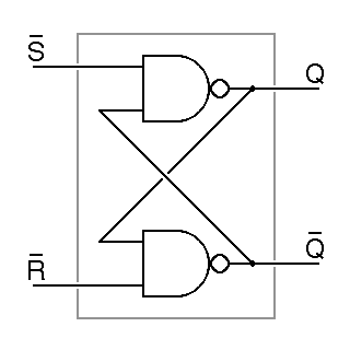
Initially, the invention of the flipflop led to the development of very high-speed vacuum-tube counter circuits. These, in turn, led to the development of more complex electronic digital logic. Prior to this, most digital logic was built from electromechanical relays. At the logic level, a flipflop can be constructed from two nand gates, as shown here:

| 
|
| Q = S nand Q | |
| Q = R nand Q | |
The names Q and Q are conventionally used for the outputs of all flipflops. This is something of an abuse in this case, because if R and S are both zero, both Q and Q will be one, despite the conventional reading that Q means not Q. We get around this by simply declaraing that we will never allow R and S to be zero at the same time. Given this assumption, it turns out that Q and Q will always settle down to opposing values.
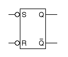
Note that in the abbreviated schematic symbol for this flipflop, given on the right in the figure, the inputs are labeled as R and S instead of R and S. The inversion indicated by overbars in the detailed drawing is indicated in the schematic by bubbles on the inputs. The outputs are still called Q and Q. This is a matter of deeply entrenched tradition more than of necessary usage.
One way of thinking about this flipflop is to focus on its description as a set of Boolean equations. We have two equations in two unknowns, and just as in conventional algebra, this means two solutions may be possible. If R and S are both one, there are two different solutions, where for the other inputs combinations, there is a unique solution, as summarized in the following truth table:
| R | S | Q | Q | description |
| 0 | 0 | 1 | 1 | forbidden |
| 0 | 1 | 0 | 1 | reset |
| 1 | 0 | 1 | 0 | set |
| 1 | 1 | 0 1 | 1 0 | hold |
Normally, an R S flipflop is maintained in the hold state, with both inputs set to one. In this state, the flipflop holds the value stored in it indefinitely. If R goes from one to zero, the Q output quickly follows, and it stays zero after R returns to one; this is why R is referred to as the reset input. Similarly, bringing S to zero sets Q to one, so S is referred to as the set input.
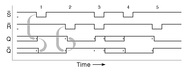
The behavior of any circuit containing feedback depends on its history. As a result, we need a way to look at the output of the circuit as a function of time and of its inputs. We do this with a notation called a timing diagram. Timing diagrams present a graph of the inputs and outputs as a function of time. Here is an example for the R S flipflop:
|
In the above timing diagram, the initial state of the flipflop is unknown,
so both outputs are shown as being simultaneously both zero and one,
signified by the lower and upper lines. No physical
logic gate will operate instantaneously, so a slight
slight delay is shown between input changes and the output changes they
cause. The first
negative pulse on S, arriving at time 1, sets Q to one and
then Q to zero;
the grey arrows in the diagram link cause and effect.
The next pulse, at time 2, is a negative pulse on
R that sets Q to zero and then
Q to one; again, grey arrows link cause to
effect. The simultaneous pulses on R and
S at time 3 cause trouble. During these pulses, both
outputs are one, but when the inputs go back to zero, the behavior of the
flipflop becomes unpredictable. Eventually, it will settle into a
stable state, but we cannot predict which state or how long it will take,
so the timing diagram shows both zero and one until the flipflop is set
to a well determined state by the pulse at time 4.
This basic flipflop and its close cousin, the RS flipflop, are found at the heart of memory technologies ranging from static RAM (S-RAM) to the bits of the registers in the central processor. RS flipflops differ from the R S flipflop only by the sign of the input pulses that set and reset the flipflop.
There are electronic memory devices that are not based on such flipflops. In dynamic memory technologies, ranging from Williams tubes invented in the 1940's to modern DRAM (dynamic RAM) and SDRAM (synchronous dynamic RAM) chips, each bit is stored as charge on a capacitor. They are called dynamic memory because this charge leaks slowly away. They are useful because because the memory controller constantly scans the contents of memory and regularly refreshes the data. Nowdays, the memmory controller is usually integrated on the memory chip, but in first-generation computers, memory refresh was actually a CPU function.
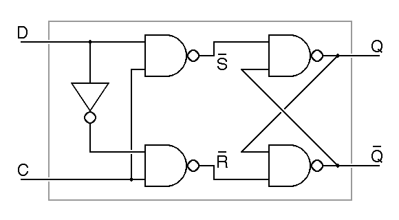
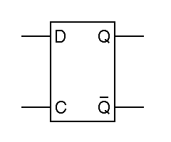
One problem with the basic R S flipflop is that we use two distinct inputs to store zero or one. To build a memory, we want one input to give the value to be stored and another input telling when to store it. Such a device, called a type-D latch, can be built from an R S flipflop plus a few extra gates:
| 
|
| Q = (D nand C) nand Q | |
| Q = (D nand C) nand Q | |
The type-D latch operates as follows. When the C input
is low, it forces the
R and S inputs to the flipflop high, allowing
the flipflop to remember a stored value. When the C input is high, the
data from the D input forces one or the other of the
R and S inputs low, setting the flipflop so that
the Q output is equal to the D input. The inputs are named D for data
and C for clock. The word clock is used because this
input is sometimes connected to a source of periodic pulses.
The term latch is an anachronism, referring to an older electromechanical
technology, the latching relay.
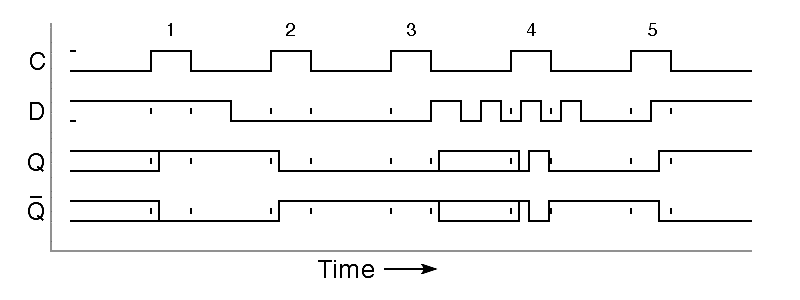
The schematic abbreviation for the D latch is shown on the right in the figure. Note that the inputs are shown without any inversion. This is becuse the Q output follows the D input, without inversion, and because the C input is normally low, with positive pulses used to tell the flipflop to store a new value. The basic D latch is not free of difficulty, as is illustrated in the following timing diagram.
|
Notice that the type-D latch is well behaved when the D input
does not change during pulses on the C input. In this case, the Q and
Q outputs change shortly after the rising edge of the C input.
This is illustrated by the behavior shown during clock pulses 1 and 2 above.
Things are different when the D input changes during a clock
pulse. In the diagram above, the D input changes at the instant that
clock pulse 3 ends, leaving the Q and Q outputs unpredictable.
The flipflop may be left in an unstable state that will settle
into a random stable state after an unpredictable delay.
After clock pulse 3 in the above timing diagram, the D input begins to
behave strangely. This has no effect on the output so long as the
C input is low, but during clock pulse 4, changes in the input pass
through to the outputs. The input change shown during clock
pulse 5 passes through to the output similarly.
Many registers within computers are implemented using type-D latches. For example, the keyboard data register for the Hawk keyboard interface would most likely be built using 8 of these. Each time someone hits a key on the keyboard, the ASCII code for that key would be clocked into these latches.
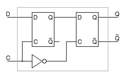
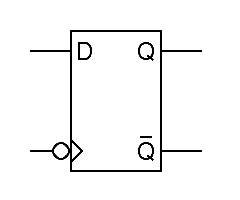
Computers of the 1950's and 1960's were commonly built using very simple flipflops, but with the advent of integrated circuits in the 1960's, a new family of flipflops came into widespread use, master-slave or edge-triggered flipflops. These are built from two simple flipflops, a master and a slave, wired in series. The clock signal is connected to these in such a way that only one flipflop can pass data at a time, so no matter what the value of the clock, so long as it is constant, no change to the input passes through to the output. Only when the clock input changes can the output change. The following example is a negative edge triggered D flipflop built using the most obvious master-slave arrangement. It is called negative edge triggered because the output only changes when the clock input changes from one to zero.
| 
|
The master-slave design shown here has two type-D
latches, the master on the left and the slave on the right. We can
substitute the details of the construction of the type D latch into the
schematic just given to see how this device is actually constructed of
nand gates and inverters. In this expanded version of the flipflop,
it is easy to see that there are two
RS flipflops at its heart, one for the
master stage and one for the slave stage.
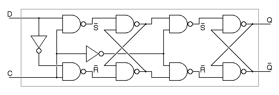
|
When the clock input is low, the master in the above circuit sees a low clock and the slave sees a high clock, so the master holds the data and it is transmitted unchanged through the slave to the output. When the clock is high, the master sees a high clock and the slave sees a low clock, so the slave holds the output constant ignoring what passes through the master. Since Q only changes on the high-to-low transition of the clock, we call this a negative-edge-triggered or trailing-edge-triggered flipflop. In the abbreviated schematic notation, the triangle on the clock input indicates edge triggering, while the bubble on the clock input indicates that the negative or trailing edge is significant.
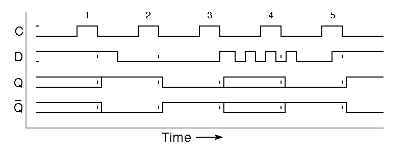
The inputs in the following timing diagram are identical to those in the timing diagram for the D latch, but because we are now using a negative-edge-triggered flipflop, the only time the output changes is when the clock input falls from one to zero. There is still the possibility of an undetermined output when the D input changes at precisely the wrong moment near the time of the negative clock edge, but aside from this remote possibility, this design comes close to being an ideal storage element.
|
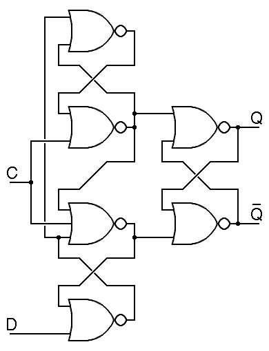
Commercial edge-triggered D flipflops were briefly made using designs close to the one here, but by 1970, optimized designs were in use. Today's designs contain the equivalent of just 6 nand gates with about two gate delays from input to output, but they are so optimized that they are hard to understand.
|
Exercises
d) Consider a circuit built using nor gates but wired identically to the RS flipflop shown here. Is the result a flipflop? If so, how is it set and reset? Is it equivalent to any flipflop discussed here?
e) Consider a circuit built with a type D latch where the Q output is fed back into the D input. What does this circuit do when the clock input is high?
f) Consider a circuit built with a negative-edge-triggered type D flipflop where the Q output is fed back into the D input. What does this circuit do each time the clock input changes from high to low?
g) How would you modify the design of the master-slave D flipflop shown here to make the flipflop trigger on the positive-edge of the clock pulse?
h) Is the modern D flipflop shown here positive or negative edge triggered?
Given a supply of flipflops and a few other parts, we can build a very simple version of the Hawk keyboard interface. We cannot hope to design a USB keyboard; the USB protocol is basically a network protocol, requiring a small microcontroller, a minimal computer, within each USB device. The serial keyboards used on early PCs are simpler, but even they require complex electronics. Here, we will assume a very simple parallel keyboard that has 9 output wires. One of these, keypress, produces a positive pulse each time a key is pressed while the other 8 hold the binary code for the key pressed.
We must also make some assumptions about the Hawk bus interface. We will assume that there is logic somewhere that decodes the memory address and delivers a positive pulse on the read FF100000 wire each time the CPU tries to read location FF100000, and similar logic for read FF100004 and write FF100004. We will also assume that the data bus for the Hawk has wires labeled D7 through D0 carrying the least significant 8 bits of the data being input or output by a read or write operation.
Given these assumptions, the keyboard data register for the Hawk can be constructed using 8 type-D latches, with the data input taken from the keyboard data lines and the clock inputs of all of the flipflops wired to the keypress line. The outputs of these flipflops must be connected to the Hawk input-output data bus when the read FF100000 line is high; this is done using special components called bus drivers, shown as triangles in the following diagram:
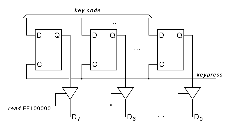
|
As mentioned in Chapter 8, a triangle with one input and one output is a a standard schematic symbol for an amplifier. The bus-driver symbol is based on this because bus drivers act as amplifiers when enabled, boosting the power enough to transmit a signal over a bus. When the bus driver is disabled, however, it is as if there were no bus connection at all. The enable signal is always shown entering the side of the triangle. When none of the bus drivers attached to a bus line are enabled, the value of that bus line is indeterminate unless a bus terminator pulls the line to a determined state; the most common bus terminators pull the bus line to one when there is no input.
Here, we have used the convention that data flows down through the schematic diagram, while control signals enter from the sides, with the central processor on the left and the input-output device on the right. It is worth noting that if we build the the keyboard data register as shown here, it is a read-only register. No matter what a program running on the central processor does, the program cannot change the contents of the keyboard data register. The only way to enter data in this register is to press a key on the keyboard.
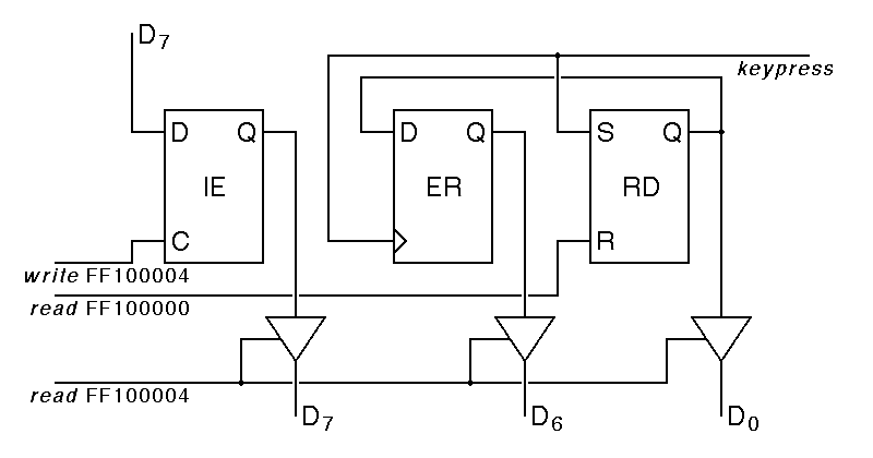
The keyboard status and control register is more complex, although it only involves three flipflops. The interrupt enable flipflop can be read and written by the central processor, while the other two have more complex behavior:
|
The keyboard ready flipflop, attached to D0, is perhaps the easiest to understand. This is a simple RS flipflop, set by a positive pulse on the keypress input, and reset by a positive pulse on the read FF100000 input, indicating a read from the keyboard data register. RS flipflops are similar to the R S flipflops we have seen except that an RS flipflop is set and reset by positive pulses on S and R instead of by negative pulses on S and R. In schematic diagrams, this is shown by omitting the bubbles from the flipflop inputs.
The RS flipflop shown for the ready bit is a significant oversimplification. What we actually want here is an edge triggered response to the keypress, so that the flipflop will be set only by the leading edge of the keypress signal. If we do not do this, the behavior of the interface will depend on the length of the keypress pulse relative to the speed of the software reading from the keyboard.
The interrupt enable flipflop is also fairly easy to follow. This flipflop is a type-D latch, with data taken from D7 whenever there is a positive pulse on write FF100004. If we wanted to build a register that acted like a general purpose read-write storage location, we would wire all of the flipflops making up that register as we have done with the interrupt-enable bit.
The error flipflop is the most complex of the three flipflops in the keyboard status register. This positive-edge-triggered D flipflop is clocked by the keypress input from the keyboard, with data input from the input ready bit. Because the keypress signal also sets the ready bit, you might think that these two bits should be the same. They are not because the error flipflop is positive edge triggered, so it samples the ready bit just as the keypress pulse begins, before the output of the ready flipflop has a chance to change. Thus, it is only be set to one when someone hits a key on the keyboard while the previous key has not yet been read by the software.
Exercises
i) How does the error flipflop in the keyboard interface shown here get reset? There is a specific event that will cause this, but only under the right circumstances. Your answer should identify both the event and the circumstances.
j) When you do a write to FF100004, what happens to bits 0 to 6 and 8 to 31 of the data written to memory? Answer with reference to the device register design given here!
k) When you do a read from FF100004, what value do you expect in bits 1 to 5 and 8 to 31 of the data read from memory? Answer with reference to the device register design given here! Note, you may have to make some assumptions; if you do so, document them!
As mentioned at the start of this chapter, typical display output devices are very different from keyboard input devices. The typical display is memory-mapped, using a display controller that constantly scans a region of memory called the video RAM or the frame buffer in order to create the display you see on your screen.
In the Hawk instructional emulator, the video RAM holds a rectangular array of characters, and we have assumed that there is hardware to display these characters on a display screen. This is comparable to the original IBM PC Monochrome Display Adapter from 1981. This is used here primarily because more complex graphics display technology requires more complex system software to perform even the simplest of graphics display functions. The basic idea of memory mapped display hardware, however, stays the same whether the hardware generates text from the display or just displays pixels.
Simple display interfaces for the Hawk occupy memory locations from FF00000016 potentially all the way up to FF0FFFFF16. The first two words of the display interface give the number of lines on the display and the number of columns. For text displays, the default, lines and columns are measured in characters, so the default text display might be 24 lines of 80 characters each. When running the Hawk emulator, these are set automatically to the size of the text window being used by the emulator, minus the size of the part of the window used for displaying the registers and memory.
In real hardware, it might be necessary to set lines and columns to match the resolution of the physical video monitor being used. Some video interfaces allow the user to set these, so you have the option of running your video display as a low-resolution display or a high-resolution display. Such interfaces (and the video monitors they drive) must be more complex than those designed for a fixed resolution.
The video RAM for the Hawk begins at location FF00010016 and consists of lines × columns consecutive bytes. In effect, the Hawk video RAM is a 2-dimensional array, with array entry zero, zero displayed at the upper left corner of the screen. Alternately, each line on the display can be viewed as a one-dimensional array of characters, and the entire display can be viewed as a one-dimensional array of lines. Each byte of the video RAM holds one ASCII character, but simple graphics displays with one byte per pixel would operate very similarly.
| FF000000 |
| ||
| FF000004 |
| ||
| FF000008 |
| ||
| FF0000FC | |||
| FF000100 |
| ||
| lines consecutive blocks | |||
| of columns bytes each | |||
Given this, the following simple function displays one character at a given row and column of the screen:
void putcharat( char ch, unsigned int col, unsigned int line ) {
    const unsigned int * plines   = (int *)0xFF000000;
    const unsigned int * pcolumns = (int *)0xFF000004;
    const char * origin  = (char *)0xFF000100;

    if ( (col < (*pcolumns)) && (line < (*plines)) ) {
        *(origin + (line * (*pcolumns) + col)) = ch;
    }
}
|
Note that, in C and C++, the declaration int * p declares p to be a pointer to an integer. Given this declaration, the expression *p gets the value of the memory location pointed to by p and assignment to *p assigns to the memory location pointed to by p. In this context, C uses the asterisk as an indirect-addressing operator. Also, the parenthetic prefix (int *) forces the following value to be interpreted as a pointer to an integer instead of whatever it would have been without this prefix. Beware, one of the asterisks in the above code is the old familiar multiplication operator, all of the others are used for indirection.
This code shows one character at the given location, after checking for coordinates outside the display area. Most users do not want the job of keeping track of the coordinates of every character displayed. From a user perspective, it should be possible to set the coordinates of the first character in a block of text and then simply output consecutive characters from that point onward. A second problem with this code is that it requires one multiply per character displayed. Given that ASCII text reads from left to right and that the display memory is also organized with the consecutive bytes of one line displayed from left to right, this code will do far more computation than necessary when displaying a string of text.
You may imagine that, with the speed of modern computers and graphics coprocessors, output speed does not matter, but it does. Whenever a the computation you are doing pushes the limits of the processor, you do not want the processor to waste time on other computations such as those involved with formatting or dispaying the results.
In the Hawk monitor, the function of setting the display coordinates is separated from the function of displaying text. This split is typical of the approach taken in many window managers. The Hawk monitor putat() routine sets display coordinates, while the putchar() routine outputs a character and updates the coordinates. These communicate through a COMMON block holding the current address in video RAM. putat() sets the address, while putchar() stores a character at that address and then increments the address. In C, we could describe this as follows:
static const unsigned int * plines   = 0xFF000000;
static const unsigned int * pcolumns = 0xFF000004;
static const char * origin  = 0xFF000100;
static char * dspptr = origin;

void putat( unsigned int col, unsigned int line ) {
    dspptr = origin + line * (* pcolumns) + col;
}

void putchar( char ch ) {
    * dspptr = ch;
    dspptr = dspptr + 1;
}
|
The code above effortlessly wraps long lines of output, relying on the fact that consecutive memory locations continue from the end of one line on the screen to the start of the next line. This code has a major drawback: It does not check for the end of the video RAM, but simply continues storing characters in continuous locations if the application tries to display more text than fits on the screen or if the application tries to use coordinates that are out of bounds.
In the code, plines, pcolumns and origin are all declared as global constants. In the SMAL assembly language, we can allocate words to hold these constants, or we could compute them from the common base address of the display area, the constant FF00000016. We will do the latter, viewing the entire display area as a structure in memory.
In the above code dspptr points to where the next character will be displayed. This is set by dspat() and also by an initializer. In the Hawk monitor, DSPINI both initializes dspptr and returns the screen dimensions. The following code does this:
        COMMON  DSPPTR,4        ; address of current display position

PDSP:   W       #FF000000       ; base address of display interface
; the following fields exist within the display interface
LINES   =       #0              ; number of lines on screen
COLUMNS =       #4              ; number of columns per line
ORIGIN  =       #100            ; row 0 column 0 of display data

        INT     DSPINI  ; initialize the display
DSPINI: ; returns R3 = columns (screen width)
        ;         R4 = lines   (screen height)
        LOAD    R3,PDSP
        LEA     R3,R3,ORIGIN    ; /* compute address of origin field */
        LIL     R4,DSPPTR
        STORES  R3,R4           ; dspptr = &(pdsp->origin)

        LOAD    R4,PDSP
        LOAD    R3,R4,COLUMNS   ; R3 = pdsp->columns
        LOAD    R4,R4,LINES     ; R4 = pdsp->lines
        JUMPS   R1              ; return
|
Exercises
l) What happens if a user of the dspch() routine given above displays more consecutive characters than will fit on a line?
m) Modify the dspat() routine so that it will not set the display pointer outside the bounds of the video RAM defined by the lines and columns registers. Trying to set coordinates outside the screen should set the coordinate to the nearest on-screen location to the coordinate given by the user.
n) Write a version of PUTCHAR that is consistant with the version of DSPINI given here.
o) Write a version of PUTAT that is consistant with the version of DSPINI given here.
When the video RAM holds pixels, not characters, text output is considerably more complex, but we can hide this complexity if we write just one key routine, the pixel block transfer routine. This is still frequently known as bitblt because it was originally developed on a system with one bit per pixel in the 1970s. Bitblt copies a rectangular block of pixels from a region of one 2-dimensional array of pixels to a region of another pixel array. The complexity of bitblt arises from the fact that the source and destination arrays can have different dimensions. For example, one array might represent the video backing store while another represents a window.
The source and destination arrays for the bitblt operation are described by their starting addresses and dimensions in rows and columns of pixels. The location in each array holding the block of pixels to be copied is described by the row and column number of the upper left corner, and the size of the region to copy is described by a height and width. Adding these up, the basic bitblt operator takes a total of 12 parameters, although it can be slighly simplified if each array object knows its own size. Given a working bitblt operator, a letter can be displayed on the screen by bitblitting it from the current font and then updating the current location by the width of the letter.
One byte per pixel is enough for a monochrome display, but for color, we need at least 18 bits per pixel, 6 each for red, green and blue. On computers with 8 bit bytes, it is common to use either 24 or 32 bits per pixel. In the latter case, the extra 8 bits per pixel are sometimes used to indicate the transparency of the pixel, with a bitblt operator that can blend transparent colors as it copies.
A fast bitblt is one of the keys to fast graphics. Because of this, major efforts have been put into optimal bitblt implementations. The optimization techniques discussed in Chapter 7 applied to the strlen operator are all applicable, since we would rather copy blocks of pixels whenever possible. Many graphics coprocessors offer fast hardware implementations of bitblt, sometimes augmented with additional transformations such as the ability to dim, blur, rescale or distort a block of pixels.
Exercises
p) Write out the full parameter list for bitblt(), assuming that arrays are described by a pointer to their first element plus separate parameters giving the number of rows and columns of the array.
q) Describe how the bitblt() operator can be used to scroll a text window up one line, in order to make room for a new line of text at the bottom of the screen.
The hardware of a video display interface is far more complex than the simple keyboard interface we described previously. To understand why this must be so, we need to look briefly at the nature of video data.
A video data stream consists of a sequence of images, repeated many times per second. For classic broadcast television in the United States, using the NTSC standard, the refresh rate was 60 half-frames per second. In conventional analog video, each frame starts with a vertical sync pulse and frames are separated by interframe gaps, called vertical blanking intervals. Each frame consists of a sequence of lines; standard television used 261 lines per half frame, with two consecutive interlaced half frames per full frame. The net resolution was 522 lines per full frame at 30 frames per second, with around 480 lines actually used for image content.
Sending interlaced half frames means that odd numbered scan lines are sent in one frame, and then even numbered scan lines in the next. The value of interlacing is that each half-frame can be thought of as a low resolution image when there is fast motion in the video image, so for fast motion, it is as if the image was being displayed at 60 frames per second. For relatively motionless images, the eye merges successive half frames to see the image at full resolution.
Just as frames are marked with sync pulses and separated by interframe gaps, lines within a frame begin with a shorter sync pulse and are separated by interline gaps, called horizontal blanking intervals. Within each line, the sequence of brightness values to be displayed are conveyed as analog voltages. Sync pulses use a special voltage called ultrablack, while blanking intervals are merely black. When video signals are sent over multiple wires, as with the VGA and SVGA connections used on many personal computers, synchronization pulses marking the end of line and end of frame are carried on separate wires instead of using an ultrablack value.
The simplest analog color video system uses 3 wires, one each for red, green, and blue. An additional wire may be used for the NTSC sync pulses, but in 3-wire video, the sync pulses were superimposed on the green signal. Analog video, in either monochrome or color, does not have a well defined concept of pixel. Instead, the video standards specified a maximum frequency for the intensity signals. Working backward from this, each scan line of an NTSC monochrome or 3-wire color signal was able to hold on the order of 640 pixels. Putting this together with the 480 scan lines typically used for image content, this explains why the VGA display adapter, introduced by IBM for the IBM PS2 in 1987, had a top resolution of 640 by 480 pixels.
The color video systems that dominated broadcast TV before the digital era are far too complex to describe here. High definition digital video standards are still evolving, but when sending HDTV signals over an HDMI cable, the basic format is the same as for 3-wire video, except that the video data is sent in digital form, with a clock signal and 3 data lines. The high data rate requires that each video data signal be separately shielded, and to provide reasonable error resistance, the video data signals are transmitted in differential form, on two parallel wires. The net result is that the 4 video signals on an HDMI connector (3 data plus clock) require a total of 12 pins in the connector.
Just as we describe the function of a central processing by its fetch-execute algorithm, we can describe a special purpose processor such as the video display controller in terms of its algorithm. Here is the algorithm a simple monochrome analog video controller might use, with one-byte per pixels and no half frames or interlacing:
unsigned int lines, columns;   /* controller interface registers */
char * origin;

video_controller() {
    unsigned int line, column;
    char * addr;

    while (TRUE) do { /* display frames forever */
        addr = origin;
        output( ultrablack );
        wait( vertical_sync_duration );
        output( black );
        wait( vertical_front_porch ); /* half blanking interval */
        for (line = 0; line < lines; line++) {
            output( ultrablack );
            wait( horizontal_sync_duration );
            output( black );
            wait( horizontal_front_porch ); /* half blanking interval*/
            for (column = 0; column < columns; column++) {
                output( * addr );
                wait( pixel_duration );
                addr = addr + 1;
            }
            output( black );
            wait( horizontal_back_porch ); /* half blanking interval*/
        }
        output( black );
        wait( vertical_back_porch ); /* half blanking interval */
    }
}
|
Notice that the above algorithm requires that
the video display controller be almost as complex as a CPU,
with its own memory address register, plus a pair of registers to count
rows and columns of the image, plus timers for the different intervals.
This processor does not need a general purpose ALU, just logic to increment
compare and initialize registers, but it does need access to main memory,
or at least, access to that part of main memory used as video RAM.
Any input-output device that directly accesses RAM is called a direct memory access device. The presence of a DMA device requires that the memory or the memory bus support multiple clients. When video RAM is used, the RAM is typically designed as a two-port memory, so that the processor can read or write memory using one port while the video controller has independent read access using the second port. If the frame buffer is in single-port RAM, the display controller typically competes with the CPU for access to the frame buffer.
If the input-output device has the potential to access any location in RAM, the general solution is to use a memory bus that incorporates bus arbitration logic. In this case, when multiple devices both attempt to access memory at the same time, the higher priority device wins and forces the low priority device to wait. When input-output devices compete with processors, the general rule is that the input-output device has the higher priority. For example, when the video controller needs to fetch a pixel, it always wins the contest with the CPU, but it always waits before fetching the next pixel, so these conflicts do not seriously degrade the CPU's performance.
Video controllers for text-only displays are more complex; typically, these include a read-only memory holding the pixel patterns for the characters. If each character is stored as an 8 by 16 array of pixels, with one bit per pixel, each line of text must be scanned 16 times in order to generate the 16 rows of pixels needed to display that line, and for each row of each character in the line, the 8 pixels of that row must be output sequentially to the video stream. Prior to 1970, the hardware to do this was very expensive, and few but the most expensive computers had video controllers and graphics output displays. The most common output device was the impact printer, either high-speed line printers or 10 character per second teleprinters.
By 1973, small solid-state memories were available that could hold one screenful of text, and text-only video displays became common. These were text-only because the extra logic needed in the controller for text-only display was less expensive than the many kilobytes of random access memory memory needed for a graphical display. It was only in the 1980's that memory became inexpensive enough that graphics displays became commonplace.
Exercises
r) Write code in the style of code given here for a pixel mapped video display controller to describe the algorithm executed by the hardware of one of the older but more complex text-only video displays.
s) Write code in the style of code given here for a pixel mapped video display controller to describe the algorithm executed by the hardware of a display controller that produces interlaced half-frames. This should scan every-other line of the video RAM for each half-frame, starting the first line of even half-frames in mid-line. The short first line of even half-frames is how the receiver knows to interlace the lines correctly.